
Sparks fly with polymers
Laser surgery for thermoplastics
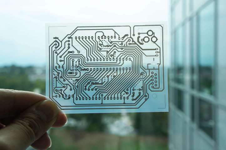
There are various ways of creating parts with plastronics, but one of the most used, and best mastered, is based on laser technology developed by German company LKPF, a pioneer in the field. Moulded interconnect devices (MID) are manufactured using a technique known as laser direct structuring (LDS). Although traditional printed circuits are manufactured using silicon and metals, MIDs are manufactured using a mix of a thermoplastic polymer and a copper-based additive. The additive is then activated using a laser which leaves copper particles on the surface of the part. The part can then be dipped in a catalyst bath to "thicken" the copper layer to the desired thickness (usually a few microns). Overall, copper is perfectly suited to conduct electricity. A mix of nickel and gold may be used for some quasi-microscopic circuits, like those in micro-wiring, which need to be extremely thin.
Staying on the topic of lasers for a moment, there is another widely-used technique called laser ablation. Converse to laser activation, the laser beam is used to make certain areas insulating by sputtering the material. It is a little like the polar opposite of the previously-mentioned technique. This method is particularly effective for creating passive antennas.
Plastics hiding high technology!
The technology has been mastered so extensively that many common objects are mass-produced using plastronics. A mundane object could in fact be hiding a miracle of technology under the surface. One of the best-known is the humble smoke detector which has become mandatory in many countries. It comprises a moulded polypropylene case containing various components. MID technology has enabled it to be simplified to the highest degree. The battery housing and the various connections are moulded directly into the item, thus forming all of the metallic contacts. "Loose" connection wires and the complex welding operations required for assembly are a thing of the past and their disappearance has helped to reduce manufacturing costs. The number of components has also dropped drastically: the printed circuit, the wires and the connectors have been replaced by conductive tracks engraved directly onto the MID.
Better yet, antennas connecting the smoke detectors to a network can be integrated by re-programming the laser. Finally, attaching a simple LED is an easy feat with this technology.
Plasma fire for all polymers
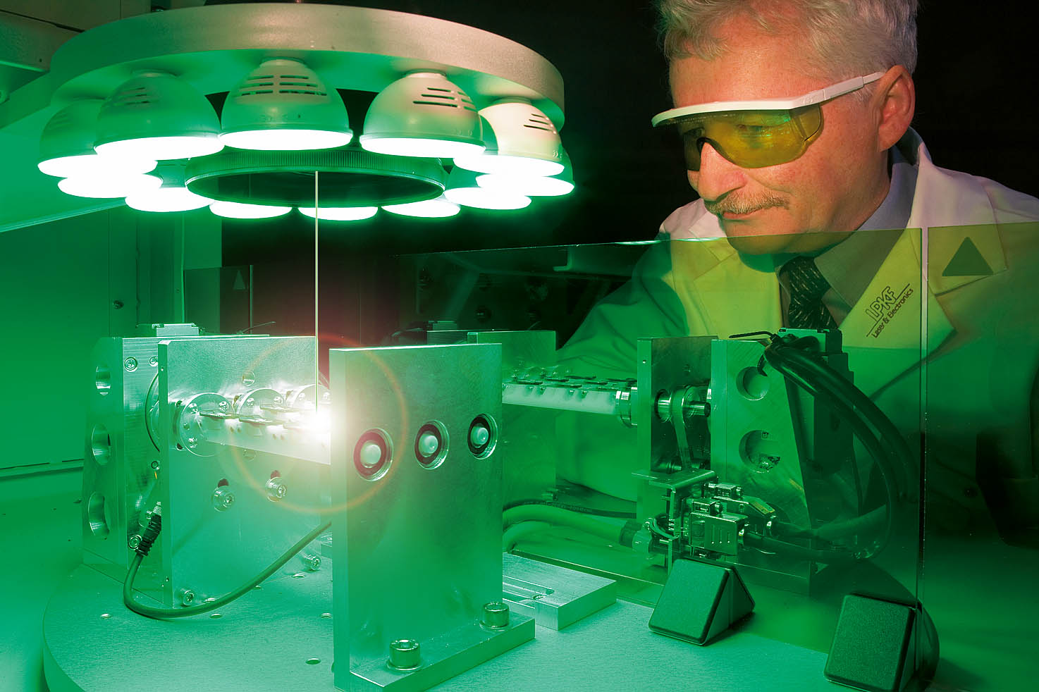
Although laser technology was the catalyst of the plastronics revolution, it still has a few drawbacks: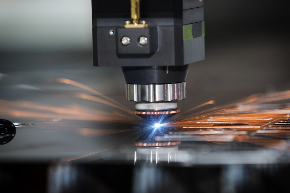 an additive has to be added to the polymer before moulding, and the part needs to be dipped in a chemical bath. Nothing so important that it could render this formidable technology undesirable. In France, S2P, a company that emerged from the European Plastics Centre, has developed a new process, christened Plasmacoat 3D, which is used to engrave circuits using a plasma torch. Quick reminder: plasma is the fourth state of matter. It is energy-rich and is made up of atoms having lost at least one electron. The Plasmacoat 3D process works by injecting a powder of a metallic material (copper or zinc) into argon in its plasma state. The resulting material is then sprayed onto the surface of the part, following, much like the laser does, the path of the future printed circuit. It adheres perfectly to the substrate, regardless of the polymer used.
The technique is of particular interest to motor vehicle parts manufacturers, in particular for designing LED lighting systems
New inks to conduct electricity
All the while, great strides are being made by researchers. The current objective is to leave behind lasers and plasma torches and insert an electronic circuit directly into a plastic part using a printer. This is a major challenge as it requires researchers to develop inks able to adhere to all types of plastics and conduct electricity. Researchers are taking a closer look at polymers and, in particular those made up of tiny carbon molecules that are better suited to conduct electricity. Although still at the pre-industrial stage, the polymeric inks already exist and are made up of polyanalynine or polypyrrole. This technology, which still needs to mature, might be used to cover surfaces a few microns wide for electrical circuits or large surfaces measuring several square metres. The inks can be deposited on various types of surfaces, whether flat or not, and flexible, transparent, robust or recyclable surfaces, among others, resulting in far-reaching types of uses and the possibility of stacking layers depending on the object.

This technology is destined to be used to design flexible smart phones in the near future.
A bright future for electricity-conducting polymers
Many industries are extremely interested in this promising technology. Obviously, it is first and foremost an avenue to be investigated for the purpose of reducing costs. A production plant would cost approximately one hundred times less than a silicon chip plant. Prototyping is also much faster since it only takes a month to create an electronic component printed on a plastic substrate from the initial design. However, the economic advantage is not the sole benefit. In the never-ending race towards weight reduction, automotive and aircraft equipment manufacturers see the possibility of designing new types of touchscreens that can combine all the main features for driver and pilot in just a few grams of material (air conditioning, entertainment, telecommunications, etc.).

The dashboard could be a decorative component by imitating an aesthetically-pleasing material, and then instantly transforming into a screen or dashboard for controlling the vehicle's main functionalities. And all of this will be made possible because researchers found a way to make a little bit of plastic conduct electricity.


