When polymers try their hand at film
Small, smaller, smallest, everything in our life is small
Miniaturisation, a creation process that enables ever-smaller products to be designed, is an old idea that has gathered increasing speed since the end of World War II and the appearance of the first transistors, which were themselves quickly soon replaced by integrated circuits. Although the rise of electronics went hand in hand with silicon, forgetting polymers would be doing them a great injustice. Without polymers, the race towards miniaturisation would have reached its apex at the end of the 20th century and the wonderful smartphone that fits in a pocket, the most essential object in this modern world, would most certainly not exist.
Polymers chip away at electronics
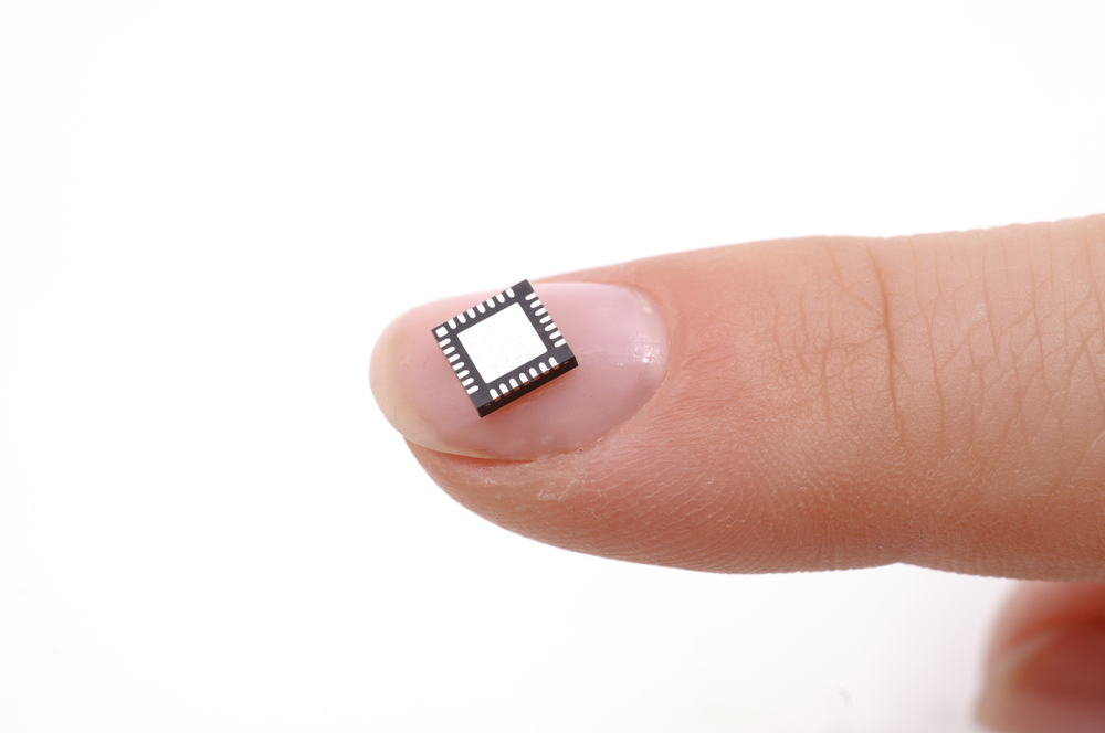
 In the early 2000s, electronic chip manufacturers were worried. According to Moore's famous law, the number of transistors in a dense integrated circuit doubles every 18 months. However, while increasing the density of the transistors on their silicon wafers, manufacturers came up a different type of limitation: the cost of the machines used to manufacture the circuits. Each new generation of chip requires a new set of equipment whose cost is increasingly difficult to absorb. In order to be able to continue offering new products, the electronics industry had no other choice but to develop higher performance and cheaper manufacturing methods. At the time, HP took inspiration from the methods for manufacturing CDs. Using a master mold, the connections are printed on a polymer surface placed on a silicon wafer, thus simplifying the manufacturing process. It may seem like nothing, but printing an electronic circuit directly onto a thin layer of plastic was quite an achievement at the time.
Plastics go on a diet
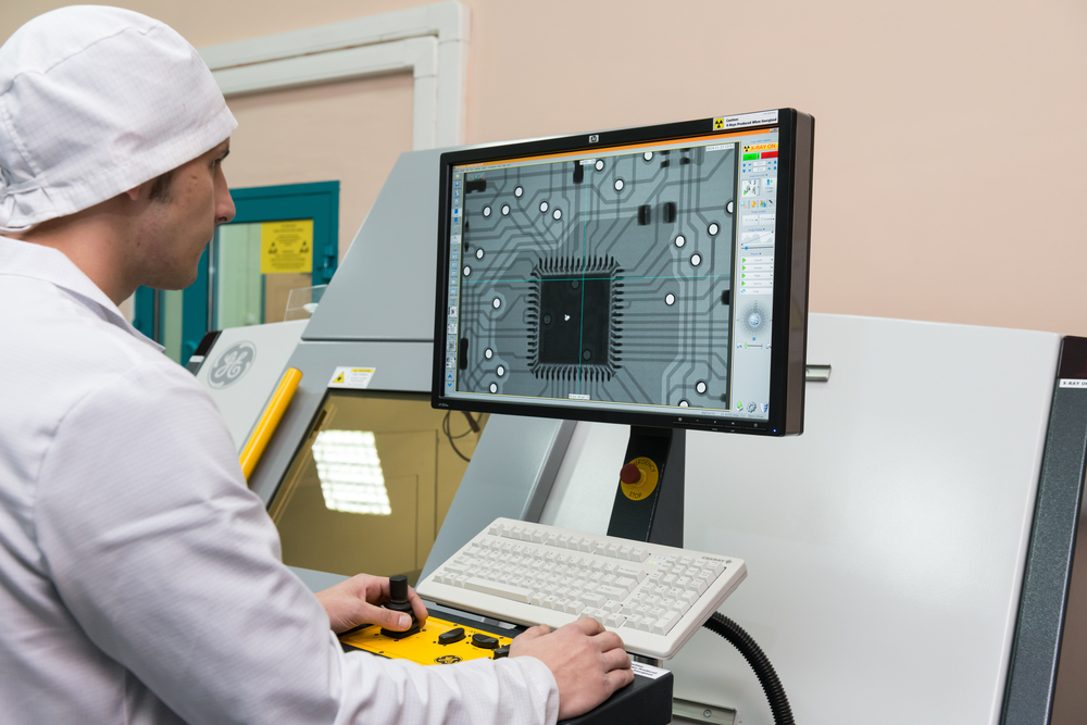 Fifteen years after the first integrated circuits were printed on a polymer, another limit was reached. This time, it would not be economic considerations that blocked technological advances, but the polymers themselves, which reached the smallest size possible of around twenty nanometres. However, in order to continue making progress, polymers needed to be thinner still. A French team at the CNRS may have found the solution. It recently developed a new combination of polymers that combines polymers from sugar and other polystyrene-based polymers. This innovative combination enables ultra-thin films measuring 5 nanometres in thickness to be produced. This copolymer has surprising characteristics: similar to a bubble of oil connected to a droplet of water, the researchers demonstrated that such a structure was able to self-organise by taking on the appearance of a film much thinner than previous generations.
Achieving this performance enables many applications in flexible electronics to be envisaged: miniaturisation of the printing of circuits, information storage capacity multiplied by six (flash memory: USB sticks are able to store six Tbits of information instead of 1Tbit), enhanced performance of photovoltaic cells, and more).
Another team also took an extra step towards the miniaturisation of electronic components by creating a plastic nanofibre able to conduct electricity. There are already carbon or gold particle composite nanotubes able to conduct electricity at such microscopic scales, but they remain vary expensive and very delicate to manipulate. Thanks to this new type of organic polymer, the race towards miniaturisation has taken a further step forwards, and the infinitely small nanomachines powered by these fibres will soon enable the creation of extremely thin flexible screens whose onboard electronics will not be visible: perfectly transparent and invisible screens and, why not, solar panels with the same characteristics.
Solar cells not to be taken lightly
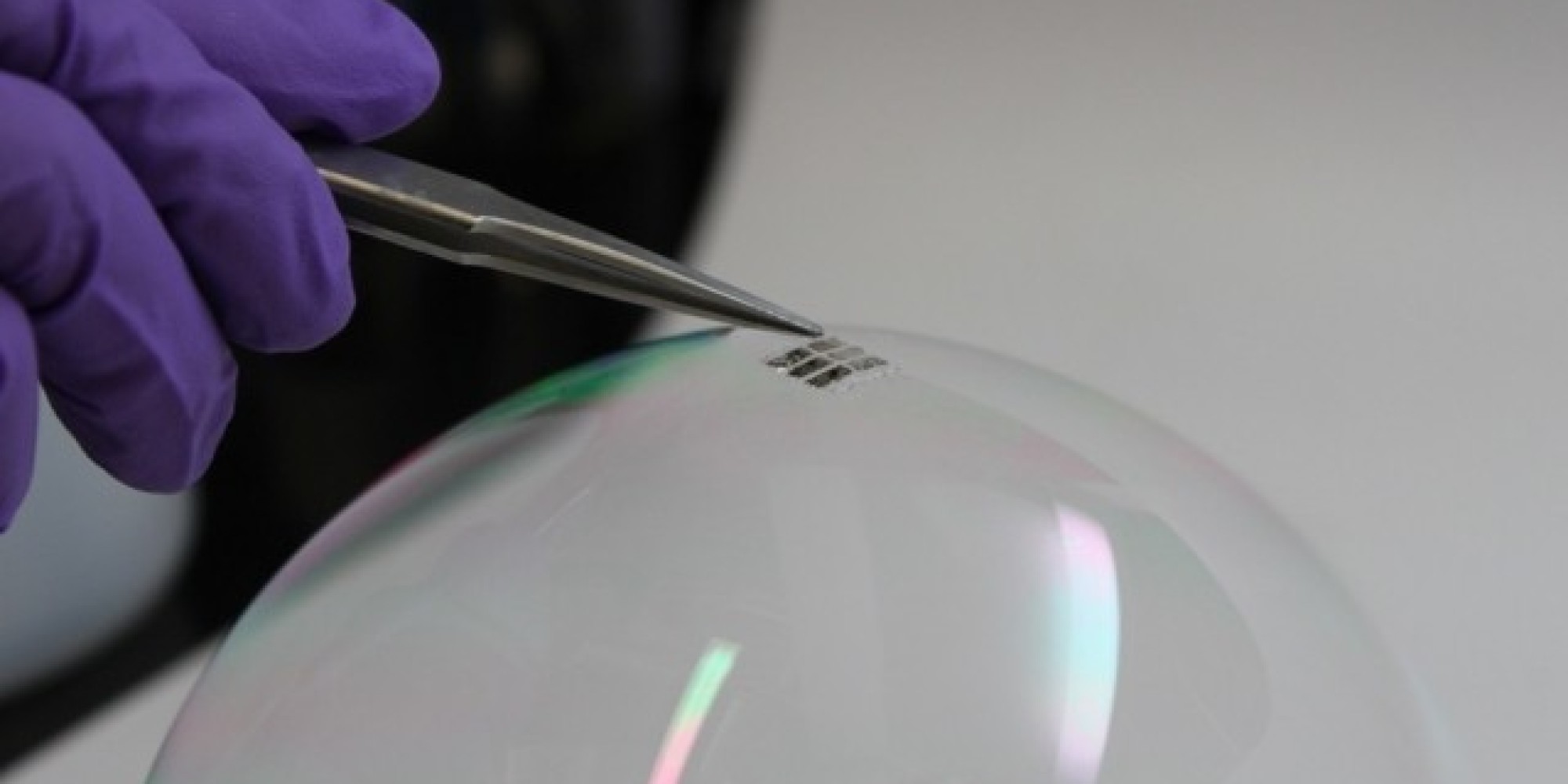 Photovoltaic cells have continued to evolve over the past two decades and the latest innovation is likely to leave a permanent mark on the industry and revolutionise our way of charging our electronic devices. We owe this technological advance to a team, at the Massachusetts Institute of Technology, which managed to design a cell encapsulated in parylene, a flexible polymer commonly used as a protective coating on medical equipment and printed circuit boards and which comes in the form of a plastic film that is ten times thinner than plastic wrap. To showcase their cell's light weight, the MIT team simply placed it on a soap bubble which, of course, did not pop under the cell's weight. The process for creating this new photovoltaic cell is carried out in a vacuum chamber at room temperature. The cell has a much higher weight/power ratio per kilogramme (around 400 times higher) than traditional photovoltaic cells.
It will therefore be possible, in the long run, to fit them on devices for which weight is a crucial consideration, such as spacecraft or helium balloons. In the nearer future, they could even be used on all of our mobile devices.
My screen under the skin
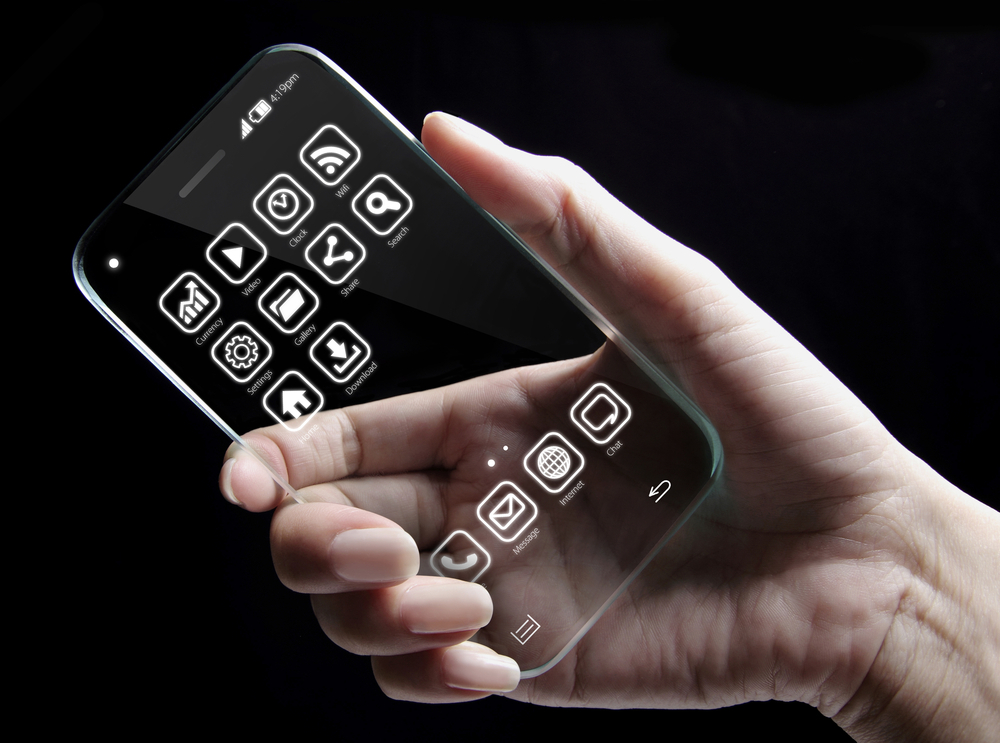
 Geeks are just a few cable lengths away from seeing their wildest dreams finally materialise: having a smart phone screen implanted under the skin without a painful procedure! This was the prediction made by a team of Japanese researchers that developed a transparent, ultra-thin and touch-sensitive electronic film that can be applied to the skin. Perfect as an invisible biometric sensor for medical and athletic use, this electronic epidermis could soon be used as a bodily screen and replaces the screens of high-tech devices. Measuring less than three microns in thickness, this electronic second skin is stretchable, flexible and entirely transparent. The plastic film includes a display system comprised of microscopic light-emitting polymer diodes, just like a screen! There is still work to be done, though, before being able to send text messages using such a screen.
In the meantime, many biometric nanosensors can be placed in the layer of plastic for the purpose of measuring various vital signs such as the heart rate, the rate of blood oxygenation, and others. Not bad, but we will have to wait a little longer before being able to watch a film on our neighbour's back.
A diaphragm in my smart phone
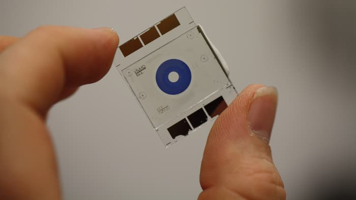
The battle of the connected devices is well and truly on. We all know about the merciless battle waged by the main smart phone manufacturers to make their devices ever lighter and more efficient. And all of this starts with the quality of the camera which has now become a crucial criterion for differentiation. Therefore, manufacturers are seeking out any innovation likely to improve photographic performance. A team at the German University of Kaiserslautern developed an electrochromic diaphragm providing the same function as the classic blade model which remains the most sophisticated and is found only on the highest-end cameras. Sufficiently miniaturised, it could be used in smart phones and would undoubtedly be highly energy-efficient. The researchers succeeded in replacing the cumbersome blade-based system with an electrochromatic polymer whose opacity can be modified by applying a low electric voltage.
Once the diaphragm's opacity has been modified, the voltage can be stopped. By placing several rings of this plastic in concentric circles, it is possible to create various brightness settings. Currently, its response time is still deemed too long, and the team is working towards making its diaphragm more responsive.
